Home
│
About company
│
International Certificate
│
Contact us
Lamination
Drilling
PTH&Panel Plating
Outer Layer
Pattern Plating
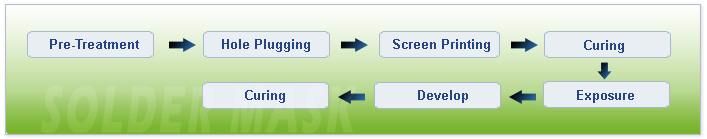
Solder Mask
Surface Treatment
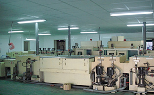
Fabrication
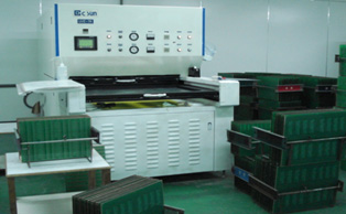
Final Inspection
Pre-Treatment & Developing
Exposure
Remark
Clearance between S.M. and Cu land: 2 mil
Spacing between SMD to deposit S.M.: 10 mil
Temporary Solder Resist
(Peelable Mask)
Copyright © 2010 quan-circuit.com.tw.All Rights Reserved.